We can provide value and satisfaction
to customers, based on Electron Beam
Lithography technology.
クレステックは徹底したマーケットイン志向の電子線描画技術を専門としたナノテク企業です


OUR BUSINESS
Crestec Corporation has established in Tokyo 1995. We delivered EB Lithography System more than 50 customers all of the world. We provide EB foundry service too. We can make fine controlled pitch L/S patterns for DFB-LD. CABL-9000C model is the best seller of DFB-LD market.
EB Lithography System
CABL-UH(130kV)series
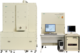
There is less forwardscatter of EB resist due to higher acceleration voltage.
CABL-UH model has more accuracy less than 10nm.
CABL-9000C(50kV)series
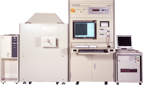
It is the best model for production of DFB-Laser diode for optical communication devices. We realize high resolution and high throughput with 50kV.
CUSTOMER LIST
We provide EB Lithography System to Universities and
research institutes for R&D purpose,
and private companies for production use too.
NEWS
MORE INFO- 2024/12/10
- Exhibition SEMICON JAPAN 2024
- We are pleased to announce that we are exhibiting at SEMICON JAPAN 2024, held at Tokyo Big Sight, from December 11 to 13, 2024. Our booth number is Hall 5 5824. We hope to see you at the site.
- 2024/12/10
- Holiday Notice
- Please be informed that our office will be closed from December 28, 2024 to January 5, 2025 due to year end holidays. We will resume operation from January 6. Thank you for your understanding and cooperation.
- 2024/07/26
- Summer Holiday Notice
- Our office will be closed for summer holidays from August 10 to August 18, 2024. We’ll resume operations on August 19, 2024. Thank you for your understanding and cooperation.
- 2024/04/19
- Japanese Golden Week Holiday Notice
- Our office will be closed for Japanese Golden Week holidays from April 27 to April 29 and May 3 to May 6, 2024. We’ll resume operations on May 7, 2024. Thank you for your understanding and cooperation.
- 2023/07/14
- Exhibition CIOE 2023
- We are pleased to announce that we are exhibiting at CIOE 2023, held at Shenzhen World Exhibition and Convention Center, China, from September 6 to 8, 2023. Our booth number is Hall 10, Booth 7D19. We hope to see you at the site. https://m.cioe.cn/en/